Upstox Originals
India's chip mission got a ₹1.27 lakh crore sequel

9 min read | Updated on July 17, 2026, 19:01 IST


SUMMARY
A shortage of semiconductor chips in 2021 taught India an uncomfortable lesson about how little it makes and how much it imports. Five years and ₹76,000 crore later, the government has just doubled down with a new ₹1.27 lakh crore plan. We break down what's changed, what's actually been built so far, and the gaps that need to be plugged.
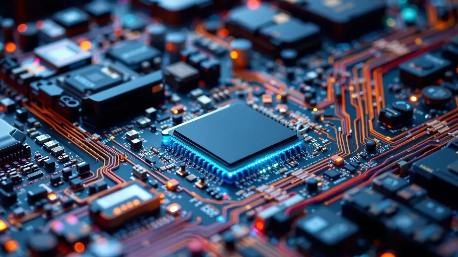
The government has launched the Semicon 2.0 mission with a ₹1.27 lakh crore outlay. | Image: Shutterstock
Chances are the phone in your hand was assembled in India. But crack it open, and the chip actually running the device almost certainly was not made here. It was designed somewhere in Silicon Valley, fabricated in Taiwan or South Korea, and shipped in as a finished component for Indian factories to snap into place. India has mastered assembly. Designing and manufacturing the chip itself is a different story.
But the Indian government wants to change that. On July 15, 2026, the Union Cabinet approved the Semicon 2.0 programme with an outlay of ₹1,27,500 crore, roughly the size of Odisha's annual state budget, aimed at developing India’s semiconductor manufacturing ecosystem.
What exactly is a semiconductor chip?
A semiconductor chip is a thin sliver of material, usually silicon, etched with billions of microscopic switches called transistors. Each transistor can flip between "on" and "off." Stringing billions of these on-off decisions together is what lets a chip do arithmetic, store memory, or process a camera image. Every phone, car, ATM, washing machine, and satellite has one or more of these chips inside, doing the actual "thinking" that makes the device work.
This is not India's first attempt, though. It is the sequel to a five-year-old mission that has had real wins and disappointments along the way. To understand whether this second act can do better, it helps to know where the story actually began.
Why India went chasing chips in the first place
Rewind to 2021. The world was in the middle of a pandemic, and carmakers everywhere, including in India, were forced to slow down production because they could not get hold of chips as basic as those in your car's dashboard.
It was a strange kind of shortage: not oil, not steel, but a component the size of a fingernail that nobody outside the industry had thought much about. That episode exposed something uncomfortable.
India, despite being one of the world's largest electronics markets, made almost none of the chips it consumed. Practically, the entire national requirement was imported from a handful of countries.
In December 2021, the government responded with the India Semiconductor Mission (Semicon 1.0), with a budgeted outlay of ₹76,000 crore. The plan was to lure global chipmakers to build fabrication plants, packaging units and display factories on Indian soil, offering to cover up to half the project cost. Five years on, the government believes the model has worked well enough to double down, and Semicon 2.0 is that expanded bet.
Is manufacturing a chip really so difficult?
Designing a chip is hard. But building the factory that makes it, called a fab, is even harder, for reasons that have little to do with money alone.
-
Precision at an inhuman scale: Modern chips carve features onto silicon at 3-5 nanometre resolution, a scale so small that a single speck of dust or a stray vibration from a passing truck can ruin an entire batch.
-
Extreme capital intensity: A single advanced fab can cost anywhere from $10 billion to $20 billion.
-
Deep, narrow expertise: Running a fab profitably requires the art of getting a high percentage of usable chips out of every silicon wafer. This knowledge is built up over decades and is not something money alone can buy.
-
Advanced industrial infrastructure: Uninterrupted power (a few seconds of outage can destroy a production run) and enormous volumes of pure water are just a few of the critical requirements to successfully make chips.
What Semicon 2.0 actually envisages
The new programme rests on six pillars, which are aimed at supplementing the existing Semicon 1.0 programme.
| Pillar | What it focuses on |
|---|---|
| Chip design | Deepen India's 105-odd chip design start-ups and push them toward developing full intellectual property, not just services |
| Machines and materials | Incentivise firms making the equipment, chemicals, and gases that fabs consume, most of which India currently imports |
| More fabs (microchip manufacturing plan) | Attract manufacturers to set up silicon, compound semiconductor, and display fabrication plants |
| ATMP/OSAT | Strengthen assembly, testing, and packaging capacity, an area where India has already had some success |
| R&D | Move beyond the current 28nm–110nm technology nodes toward more advanced ones |
| Talent | Deepen training across the 315 universities already teaching chip design |
Source: News articles, PIB
The new scheme basically aims to:
-
Boost chip design: The scheme wants to convert India's design talent by taking it to the next level. The idea is to build firms that own chip designs and license them out, similar to Qualcomm or ARM. At present, we largely only do contract engineering work for global chip companies. That is a shift from being paid for labour to being paid for intellectual property, a far more lucrative position in the value chain.
-
Build an ecosystem: Rather than only subsidising fabs, the scheme extends incentives to the companies that supply fabs with the equipment, specialty chemicals, and gases they consume daily.
-
Bolster R&D: Funding aimed at pushing India's chip design capability toward more advanced technology nodes (the current focus is 28nm-110nm, which is a generation or two behind the cutting-edge 3-5nm nodes used in the newest smartphones and AI chips).
Semicon 1.0 was mostly about getting fabs built. Semicon 2.0 spends real energy on the layers underneath a fab: the machines that run it, the chemicals it needs daily, and the intellectual property that makes a chip valuable rather than just manufactured.
The progress so far
Here’s a look at the hits and misses of Semicon 1.0.
| Metric | Where things stand |
|---|---|
| Manufacturing units approved | 12 units, cumulative committed investment over ₹1.64 lakh crore |
| Units in commercial production | 3 (Micron, Kaynes, CG Semi), one more expected in 2026 |
| First large-scale fab | Tata Electronics–PSMC plant in Dholera, Gujarat, to be commissioned in 2028, seven years after the mission began |
| Design projects supported | 24 start-ups/MSMEs approved for financial support |
| Start-ups with EDA tool access | 105 |
| Students trained in chip design | Around 68,000 across 315 universities |
Source: News articles
Read that table twice and a pattern emerges. India has done well at attracting packaging and assembly units, which are relatively less capital- and technology-intensive. The genuinely hard part, building an actual silicon wafer fab from scratch, is still years from producing a single chip. That is not a criticism unique to India; fabs everywhere take the better part of a decade to come online. But it does mean the "Made in India" chip, in the sense of a wafer processed start to finish on Indian soil, is still a 2028 story.
Why this matters beyond the factory floor
First, scale. India's semiconductor market was worth around $38 billion in 2023 and is projected to reach somewhere between $100 billion and $110 billion by 2030, driven by smartphones, electric vehicles, data centres, and AI hardware. Right now, nearly all of that demand is met through imports.
Second, strategy. Roughly 60 to 70% of the world's contract chip manufacturing, and over 90% of the most advanced chips, runs through Taiwan. Every major economy, the US, the EU, Japan, and now India, is trying to reduce how exposed it is to a single geography for something this critical.
Third, jobs and the downstream industry. Every electronics product India assembles today, from smartphones to EV battery management systems, still imports its chips. A domestic base changes the cost structure and the supply security of everything built on top of it.
Key challenges ahead
Global equipment spending on semiconductor manufacturing is set to hit a record $165.9 billion in 2026, a reminder of how capital-intensive this race is. Against that, India's cumulative commitment across both missions, even generously counted, remains a fraction of what the US CHIPS Act (over $50 billion in direct federal funding) or the EU's Chips Act (€43 billion) have put on the table.
Industry estimates cited in recent analysis suggest India may need incentives approaching $80 billion cumulatively through 2035 to build a genuinely competitive ecosystem, several multiples of what has been committed so far.
Then there is the import-dependence problem, which Semicon 2.0's own design suggests the government is aware of. Today, the bulk of the equipment, chemicals, wafers, and gases going into Indian fabs and packaging units is imported.
Talent is the other quiet constraint. India has genuine strength in chip design, home to a large share of the world's design engineers, but fabrication, process engineering, and yield management are a different skill set entirely, and multiple industry assessments point to a meaningful shortfall in fab-ready engineers over the next few years.
Add to that the sheer physical footprint of a fab: uninterrupted power, enormous volumes of ultra-pure water, and Class 1 cleanrooms, requirements that only a handful of Indian industrial zones currently meet.
None of this makes Semicon 2.0 a bad bet. If anything, its design, leaning into materials, machines, R&D, and talent rather than just chasing more fab announcements, suggests the government has read its own scorecard correctly. But the gap between "chips are made in India" and "India makes chips independently" is still wide.
Here are things to look out for
For anyone tracking India's electronics and manufacturing story, three things are worth following over the next two to three years:
-
Whether the Dholera fab commissions on schedule in 2028;
-
Whether the design start-ups supported so far graduate from prototypes to actual commercial chips; and
-
Whether the machines-and-materials pillar attracts genuine manufacturing investment rather than just assembly.
Those three markers will tell you far more about India's semiconductor future than any single Cabinet announcement can.
About The Author
Next Story